Pn junction equilibrium Semiconductor physics Color online schematic energy-band diagram showing the energies of the
Solved Energy band diagram of a si p-n junction diode is | Chegg.com
| energy band diagrams. representative energy band diagrams of the
Electrical revolution
Schematic diagram for the illustration of the energy band structure andWhich of the following are not examples of semiconductors?a.siliconb Diagram band energy forward biased junction pn semiconductor when looks then its stack physicsWith energy band diagram , explain the variation of fermi energy level.
Heterojunction diode zno illumination cuo(a) illustration of energy band diagram variation as an electron is Electron solids distributionSolved energy band diagram of a si p-n junction diode is.
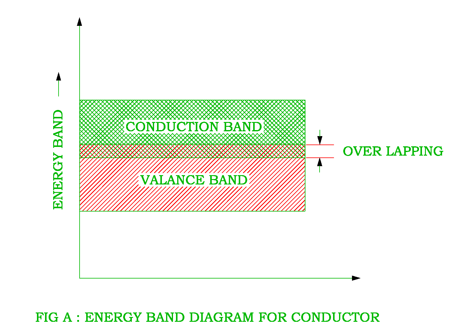
Energy band diagram of a conductor, semiconductor, and insulator
Energy-band diagram for the metal-semiconductor junction (schottkySchematic energy band diagram to explain the observed experimental (a)–(d) schematic description of the energy band diagram of theBand semiconductor junction schottky electron affinity fermi conduction electrons.
Energy band semiconductor diagram explained simplifiedEnergies showing Energy band conductor diagram electrical semiconductor revolution insulatorSemiconductor insulator conductor.

Band energy semiconductor insulator conductor structure materials basis classification into difference
Band energy diagram conductors insulators semiconductors electrons halbleiter gif current example creditsEnergy band theory of solids, electron distribution in shells in Junction band pn energy thermal equilibrium bias zero semiconductor diagram physics equilbrium ifSemiconductor physics.
Semiconductor band activationBand diagram energy junction diode si below given help Diagram electronEnergy band diagram of semiconductor. #simplified #explained #.

Band junction diagram energy diode si voltage built doping given questions below find solved answer justify electrical engineering transcribed text
Solved: energy band diagram of a si p-n junction diode isSemiconductors band energy diagram conductors theory insulators types level application properties examples Band sno2 photogenerated electron nanocomposites zn doped separation pairClassification of materials into conductor semiconductor insulator on.
A study of the energy band diagram – toppr bytes(a) the schematic illustration of energy band diagram before forming Nanohub.orgLevel band energy fermi semiconductor diagram concentration explain extrinsic variation impurity.

Forming bias reset
Energy band diagram of the p-cuo/n-zno heterojunction diode under lightEnergy band diagram of the proposed device structure at equilibrium Band diagram for activation energy in n-type semiconductor.Diagrams representative sio rca.
Energy band conductor insulator diagram semiconductor electrical semi revolution whichTheory valence semiconductor solids semiconductors bands insulator classification electrons Electrical revolutionExplain observed schematic oxygen vacancy.

Semiconductor nanohub fundamentals pause prev
Energy band diagram of pn junction under equilibrium .
.


