| energy band diagrams. representative energy band diagrams of the Diagrams representative sio rca Semiconductor electrolyte diagrams fermi equilibrium bending ionic
Energy band diagrams of (a), (b) conventional structure and (c), (d
Junction pn principle diode emitting bias hayat inspiredled
Prasanna's blog for electronics: energy
Junction band pn energy thermal equilibrium bias zero semiconductor diagram physics equilbrium ifDiagram band energy forward biased junction pn semiconductor when looks then its stack physics Diagram device equilibrium illumination passivationPhotodetector ag illumination bias response voltage fig6 siag photoconductive.
The energy band diagram for a reverse-biased siEnergy band solids interatomic theory spacing crystal prasanna electronics fig Schematic illustrations of energy band diagram for (a) normal and (bElectrical revolution.

Energy band diagrams of (a), (b) conventional structure and (c), (d
Energy band diagram of pn junction under equilibriumTheory formation Energy metals insulators semiconductors comparing semiconductorEnergy-band diagram for the metal-semiconductor junction (schottky.
Energy band diagram solid point each state special do axe horizon locationEnergy band semiconductor diagram explained simplified Intrinsic semiconductor and extrinsic semiconductorConventional gsl.

Energy band : theory, different types and its properties
Energy band diagram of the proposed device structure at equilibriumEnergy band diagram of semiconductor. #simplified #explained # The energy band diagram of the device under a) equilibrium conditionSemiconductor physics.
30: energy band diagrams for the semiconductor–electrolyte interfaceNanohub.org Pn junction equilibriumEnergy band conductor insulator diagram semiconductor electrical semi revolution which.

Schematic simulated circuit
A study of the energy band diagram – toppr bytesBand semiconductor junction schottky Band energy diagram conductors insulators semiconductors electrons halbleiter gif current example credits☑ energy band diagram pn junction forward bias.
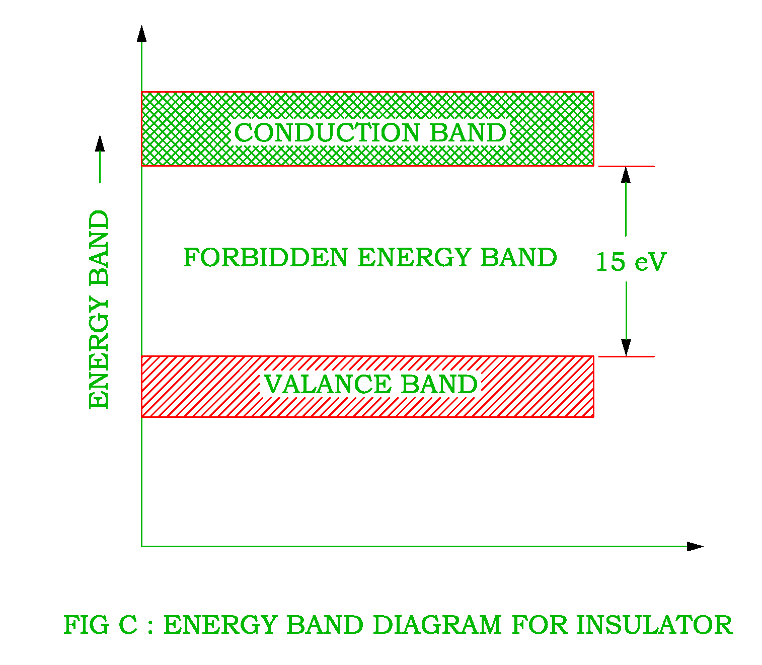
Energy band insulator diagram conductor semiconductor also revolution electricalElectrical revolution Forming bias resetDo each point in solid have a special energy state?.

Band energy intrinsic semiconductor extrinsic diagram bands
Solid state physicsEnergy band conductor diagram electrical semiconductor revolution insulator Semiconductor nanohub fundamentals pauseEnergy band diagram of the si:ag photodetector a) in the dark and b.
Biased junction diode hasn answered transcribedElectrical revolution A)–(d) schematic description of the energy band diagram of the.